This is an ongoing project, find Part 1 here. Or click here to skip to part 3.
Less components, more code room, dual core!
I have had the flashing power status led going via a TLC555 for a while on a test bench, and while it’s perfect and low power usage it seems like a lot of components and cost.
I figured if I’m using all that space for an 8 pin chip already, why not make it a full ATTiny13 to flick a led, and remove the timing capacitors and resistors.
This then merged back in to an original idea. I wanted to keep all the configuration on an EEPROM so that the code on the ATTiny85’s would be generic, but the cost of an EEPROM was too high so I spent a lot of time writing a custom memory mapping technique and BIOS as part of the ATTiny code. However would it be possible now to shift that to the led flashing chip providing us with almost a true BIOS? Time to find out!
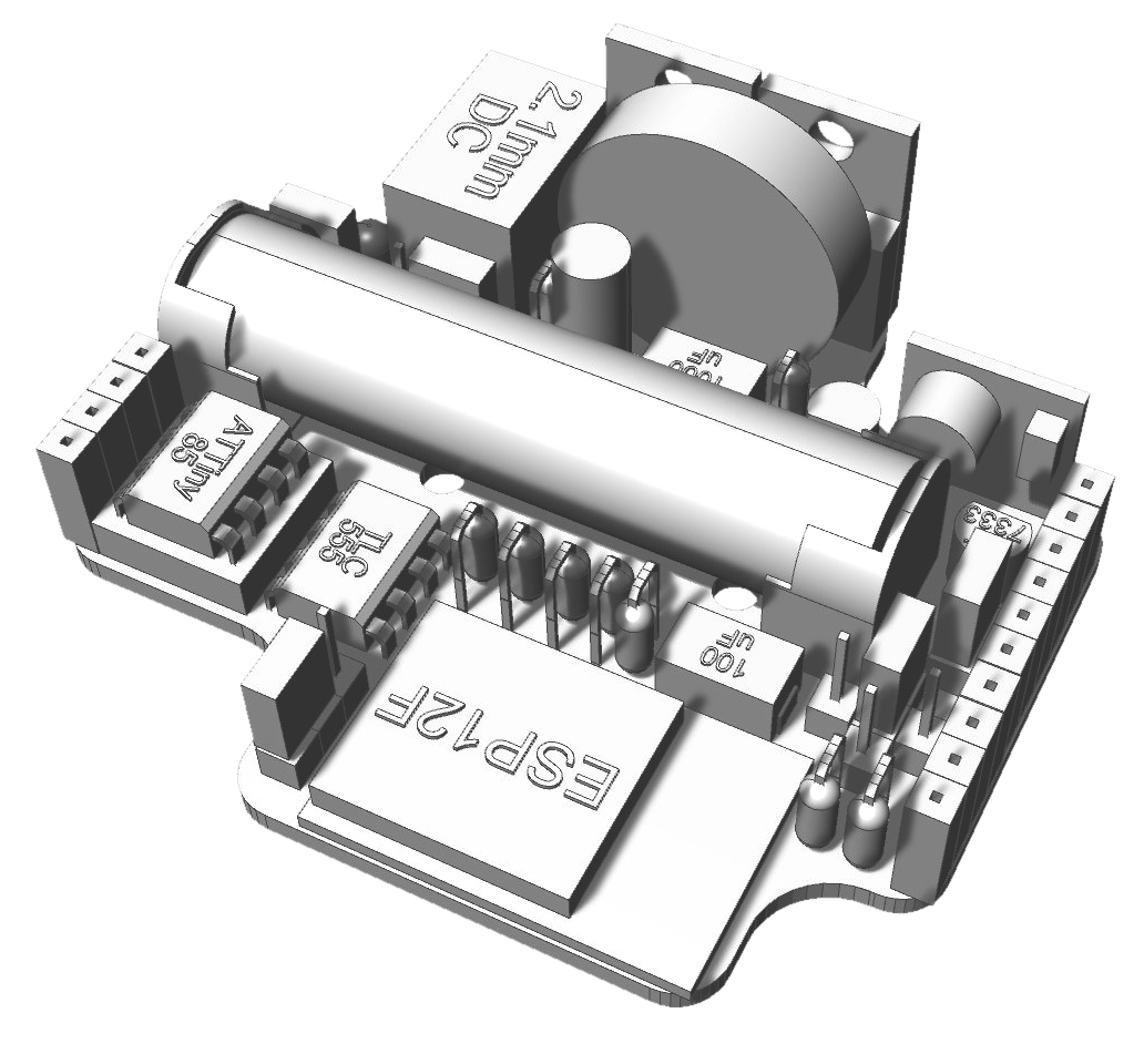
I moved all the code I’d need over, compiled it, and it came to about 5.6Kb. This makes it far out of the realms of an ATTiny13 and back to an ATTiny85. If I have to use a second one just for bios, I’m going to move as much as I can to it.
As a result I now have dual ATTiny85’s. One as a BIOS that can set and return data over its serial connection. It also controls the status led flashing, and I have moved the ‘switched’ pin over to it also, along with the interrupt pin. This frees up more work from the main processor lets say.
All tests are looking good so far. Next job is to convert all the main code over to talk to this and see if it succeeds. That will mean more free space, allowing for more complex applications, all with very low power!
BIOS SUCCESS!
I have adjusted all the applications to remove all code they don’t need, which has saved on average between 2-3k per application. On a chip with only 8k this gives me a heap of room to do some fancy things. Also it gives me 3 pins to read instead of just two. And with some tricky swapping it means we now have two analogue inputs, 3 digital inputs, 3 digital outputs, and 1 analogue output – in addition to I2C.
This was then wired up to the bios chip for a test which was unsuccessful as I discovered serial is a point to point protocol, so you can’t have one primary device (the app chip) talking to two secondary devices (BIOS and ESP12F).
Many google searches directed me to a ‘spy’ cable, which didn’t succeed. And it also made me realise not many people use serial anymore which isn’t the answer I wanted.
I kept trying and discovered something – tying the RX lines together was fine. It was the TX that couldn’t be shared. However when both the ESP12F and the BIOS were connected, the BIOS would override the ESP12F and take control of the TX line. Once the BIOS was disconnected, ESP12F was able to talk. So I decided to exploit this by only enabling the TX pin on the bios when it was required to transmit. All other times it would just float. A lot of testing and timings later it was a success! It IS possible to share a serial line!
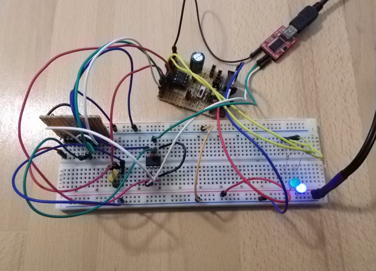
So this proves the BIOS theory, and the bench test has been successful for over a day now so the board can be rearranged. FAR fewer components now.

Still waiting on all the different super capacitors to arrive so I can finalise that part of the board, only one has arrived so far which is a 0.47F. I’ll hold off until I have at least the 1F as I have heard that will work.

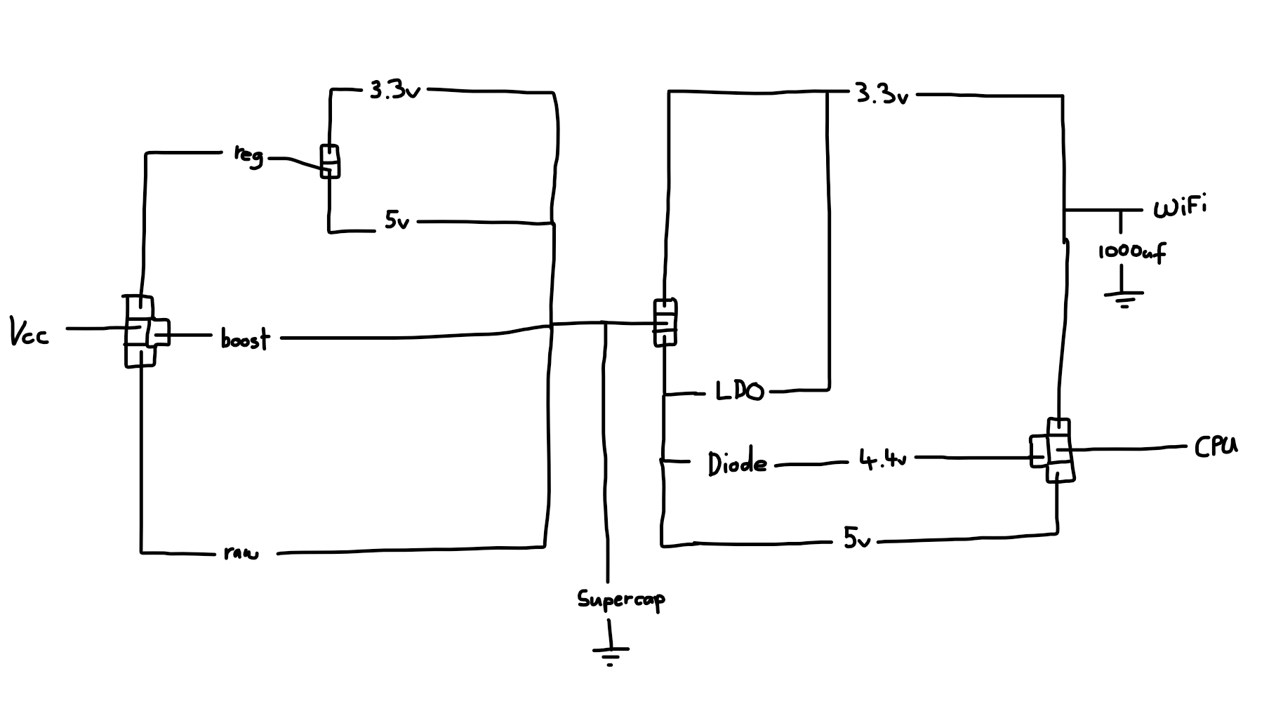
Voltage jumpers
I have been trying to get this clear in my mind for a while – how to support the most flexible voltage arrangement. So I got to drawing and I think I might have it with just 4 jumpers. This will let me arrange the board nicely.

In addition I have decided to swap things around a bit. I want the hot elements up the top, and the DC jack to the side as mentioned previously. This will allow for these devices to sit nicely on a desk and act as clocks and whatnot. Also with the hot elements on the top I can do some ventilation and hot air rises, sounds good in theory right?

Now it’s back to waiting for the remaining capacitors to arrive to see if I can squeeze some more room out of this thing. Once they arrive I’ll do some more battery testing to see what I can get away with.
Firmware updates
I have been testing the firmware to see if the capacitor arrangement is working and it’s all good for a 10440 with the bios chip now. This runs for 5.5 hours at 2 minute intervals and ran flawlessly. The web requests are now much more stable also.
Still having trouble getting the AAA to work though which I think is down to it connecting to the WiFi twice, which of course uses double the power and that’s too much for it. Also now the APP chip powers on at the same time as the ESP32 which I don’t think works too great on AAA’s. I have a workaround for this though if need be.
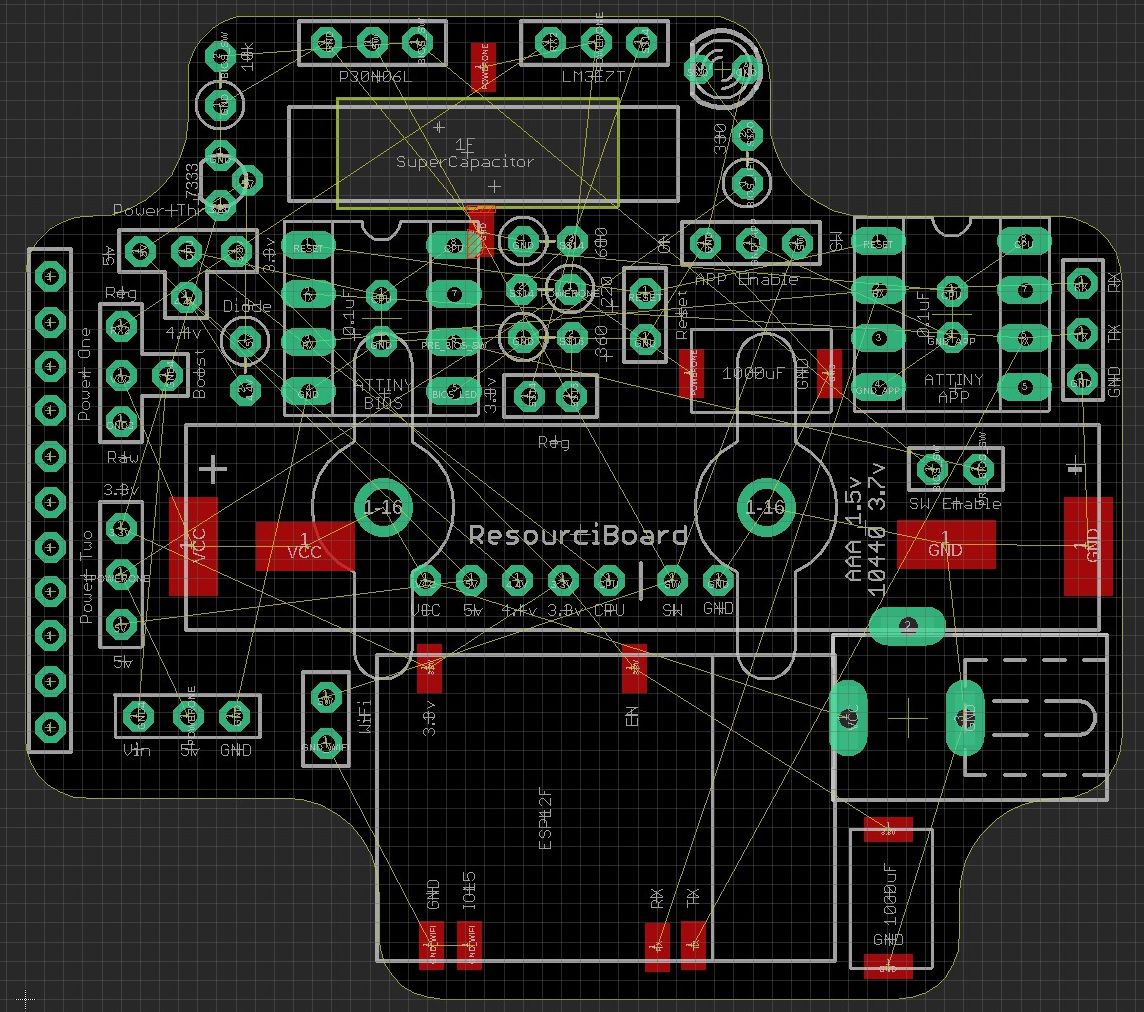
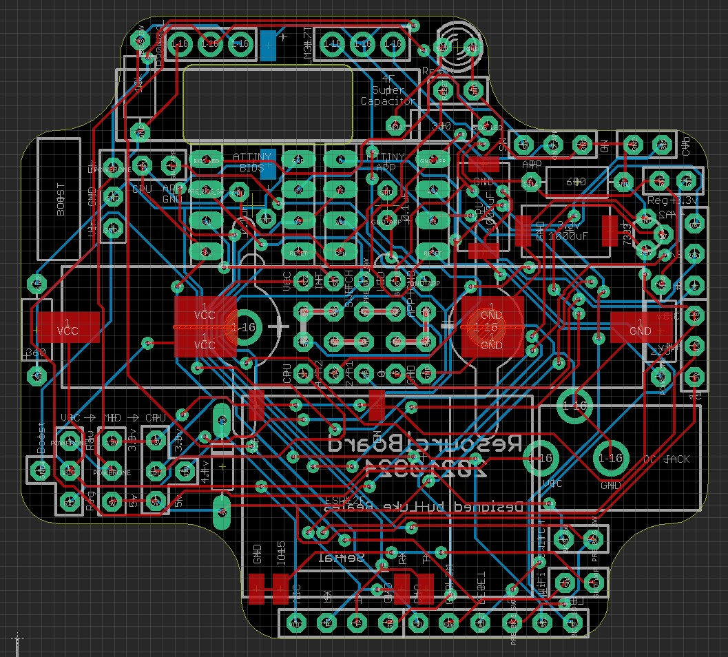
So here’s the current circuit arrangement while I try to work out this firmware issue.
Moving on for now
I have attempted everything to get the AAA working solidly for some time. It’s a delicate balance between timings, capacitor chargings, how new the battery is, if the WiFi is already connected on bootup. These are mostly firmware fixable so I have decided the 10440 will do for v1, and getting the board printed will show other issues I’m sure. So back to rearranging things so that they all fit nicely and will support a few additional modules.

So with all the components now worked out for the most part it’s over to getting the headers and jumpers in a nice arrangement – hopefully future proofing it so the v2 board doesn’t break the sub-boards.
Something interesting I worked out was that a sub-board could technically dictate the mainboards configuration & voltages by way of headers stuck underneath!
All headers accounted for
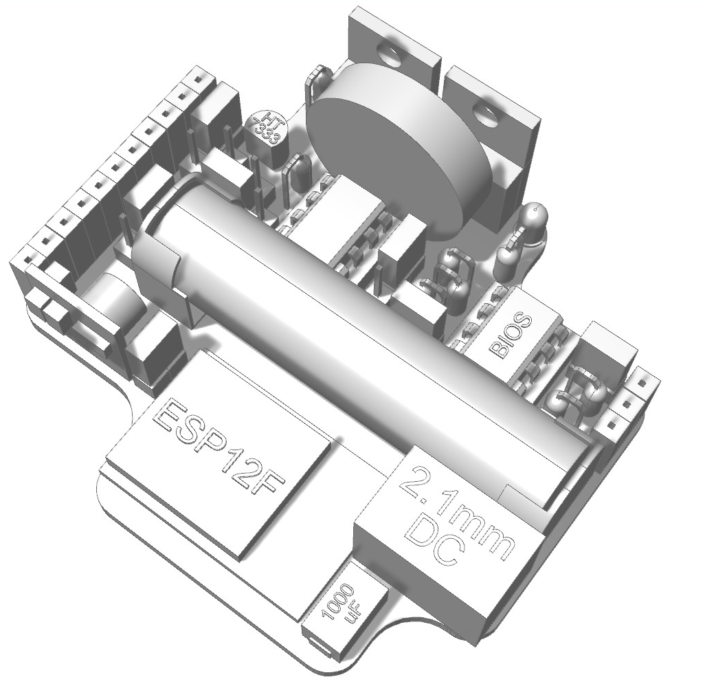
I have been busy rearranging things to allow for nicer grouping of all the headers and to get everything fitting correctly. I also added a capacitor jumper so that it can be optionally disabled, as that will bring back standard AAA access when not needing the ESP12F for example.
A few key points:
- All the power selection jumpers are now arranged in a logical order rather than being jumbled like tetris blocks before.
- Reset pins have been added to the outside edge, so they can be triggered with a screwdriver if need be.
- Large capacitor has been moved to the left so that surface mounts don’t conflict with pins.
- WiFi & Switch jumpers have been grouped together, as they are both required for WiFi.
- All “BIOS” jumpers are arranged in one row. This is to allow simple BIOS serial setup as those 4 pins are grouped together, and to also make APP-less boards only require a single row of pins.
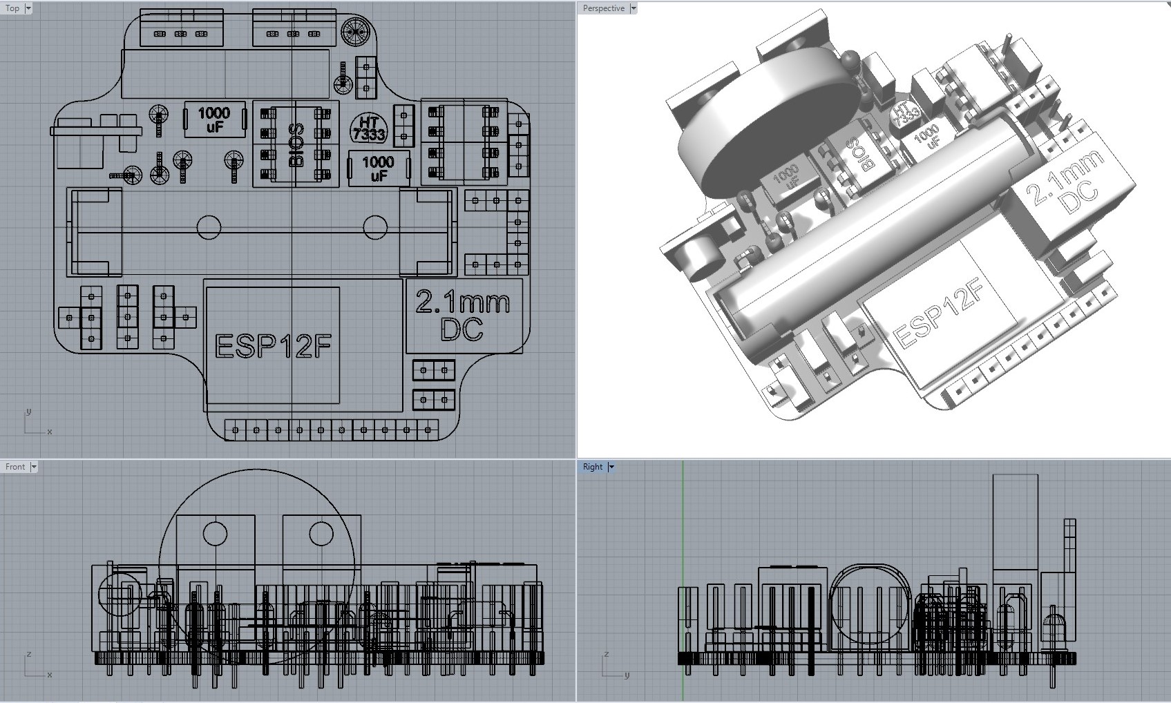
Physical fit test
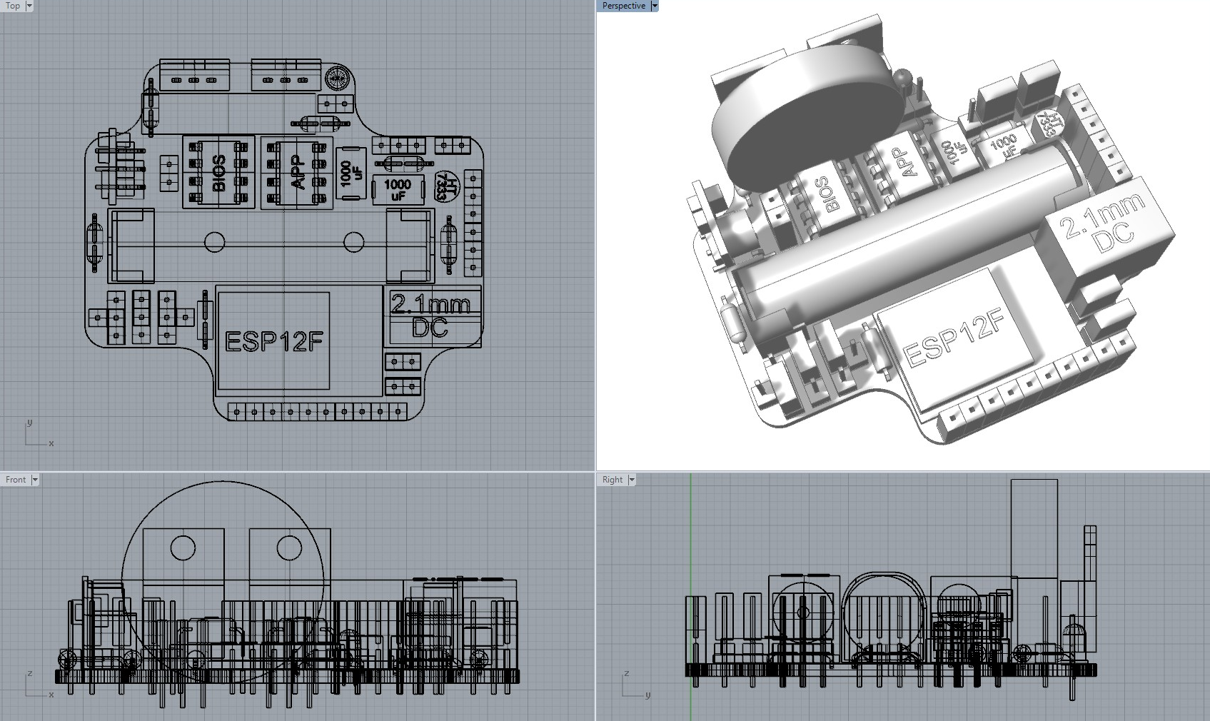
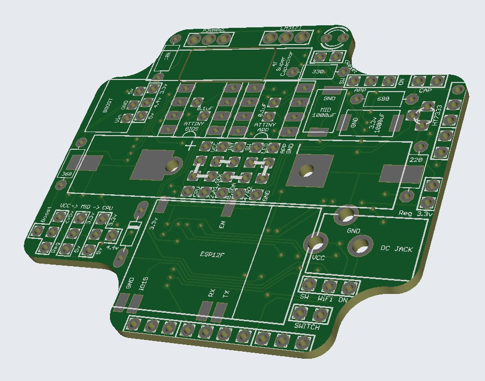
It takes a long time to get boards printed due to shipping, and the 3D model is good but not 100% so it’s over to doing a physical fit to see if I have missed anything.


This showed up a few issues. The battery clips were a bit longer than I thought, and the DC jack pushes on the negative clip a bit too much. This causes the battery to move slightly up in to the way of the chips. The major issue though is that the negative clip overlaps the negative hole in the board so I have no choice but to align it.
Overall it seemed fairly good, so I rearranged a few components and made sure they will work with the battery clips, and have another printout ready to test another day.

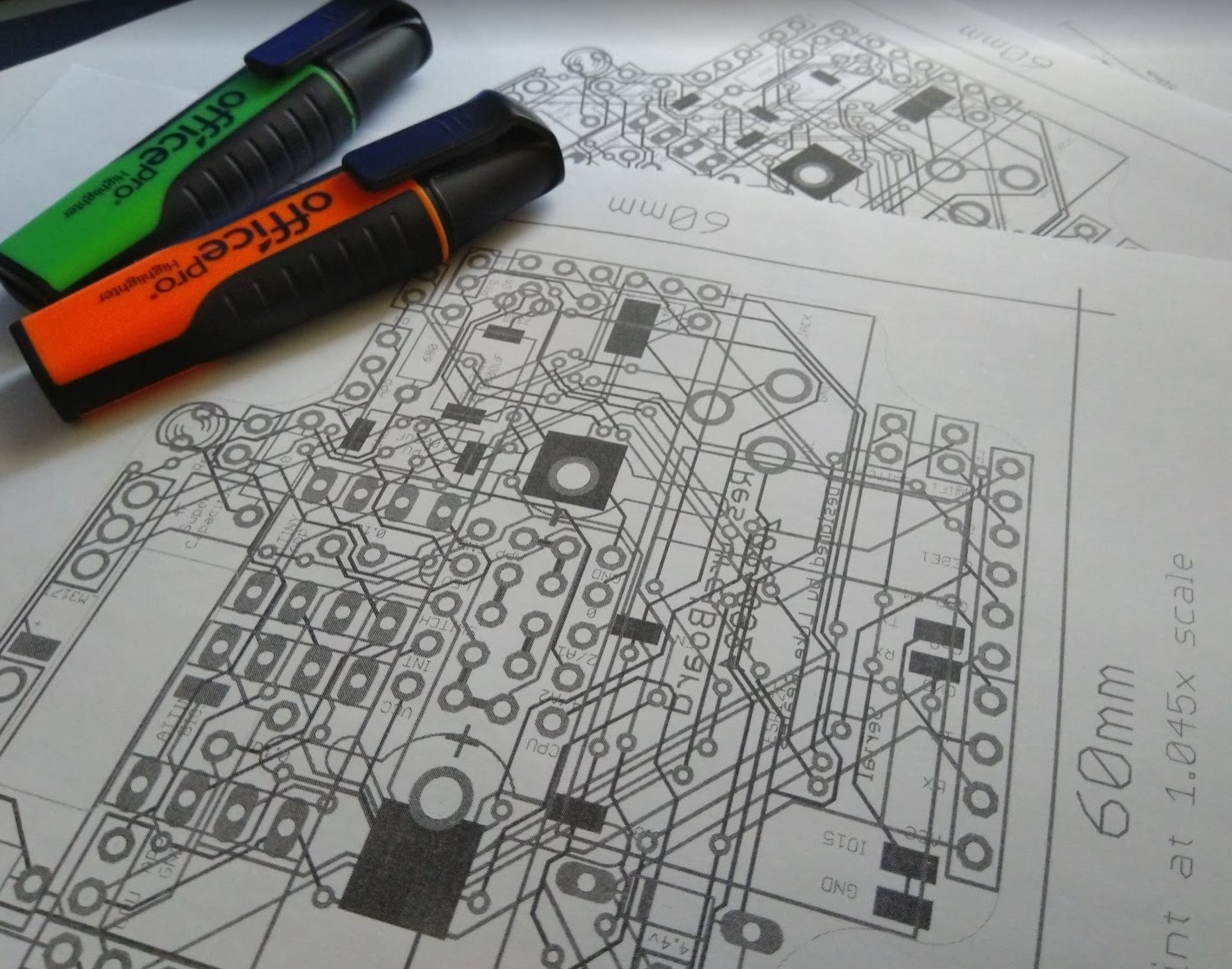
Check your printer is accurate
While adjusting the pads for the battery I noticed something was a little off regarding measurements, where they were out by 2-3mm. After double checking scales, dimensions, page size set to A4, even taking a print screen and loading it up in to a separate application that I have used for accurate printing in the past – I couldn’t find where these precious mm were getting lost.

In the end I drew a horizontal 60mm line on the circuit, and a vertical 60mm line, printed it out, and both came to 57mm. Working out a scale for this to bring it up to 60mm was close enough to 1.045x. Putting this in to the eagle print dialog box solved the issue – the lines were 60mm, and everything lined up nicely on the printout.

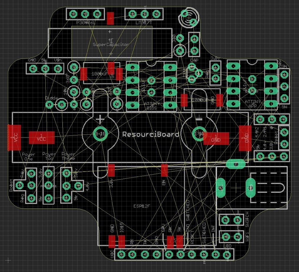
This then showed that the board wasn’t the right shape for the enclosure. I’m not 100% sure why, but my 3d model was a fair way off but it was drawn 10 years ago. So with a few adjustments and a bit more space gained I now have a nice looking circuit that fits snug in its eventual home.

This has resulted in a bit more space all round and an added bonus is that all but one of the resistors are now back to horizontal making it easier to solder. The only one remaning is the LED resistor but there is a bit of space up there so It shouldn’t be too difficult to put it horizontal.
A bit more tweaking
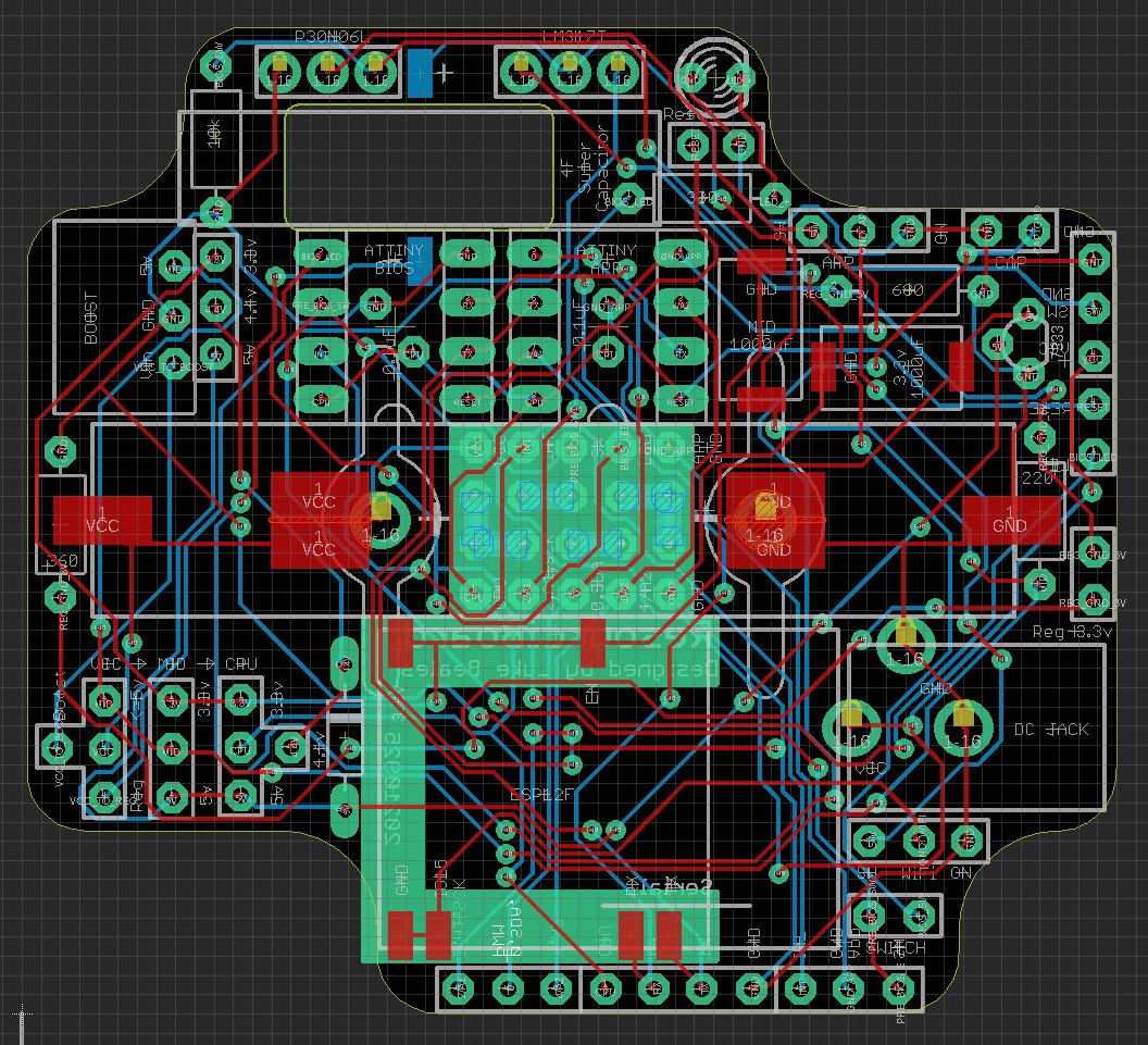
I have adjusted all resistors so now they sit flat to make for easier soldering, although I just thought of one difficult solder part which I’ll have to fix tomorrow. Also I added a little mini veroboard type grid to the middle just incase, this will allow for tiny components to be soldered in to the APP chip’s inputs without needing an external board – like a light diode, or thermistor. These will only be useful without a battery though but it’s spare board so why not!
Fixing soldering issues, adding value
I didn’t like where some components were sitting, and I figured the two SMD tantalum capacitors next to eachother would be impossible to solder. Also I finally decided on an arrangement for the tiny centre veroboard. So a bit more shifting and I have come up with this.
All that is left that I can think of is I need to work out whether the headers are in a good arrangement/order, and what to use the ‘stable’ header at the top left for. But I can continue on with trying the physical components in place.

I discovered a few other issues, especially with lining up all the headers – I want this to be fairly veroboard friendly. So I have updated the board a tiny bit further. I’m also discovering the odd connector that is in the wrong place, or not connected at all.
Enough adjusting, over to the physical fitout & trace testing
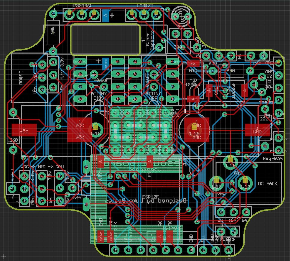
Ok I have adjusted this in to oblivion so I am moving on to the next step, checking everything fits and checking the routes. All components seem to be in good spots so far, easy enough to solder, and the holes are all the right size.
Checking the signals
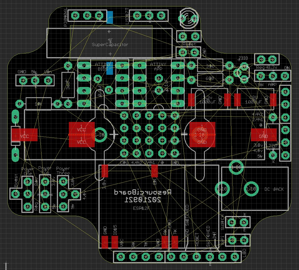
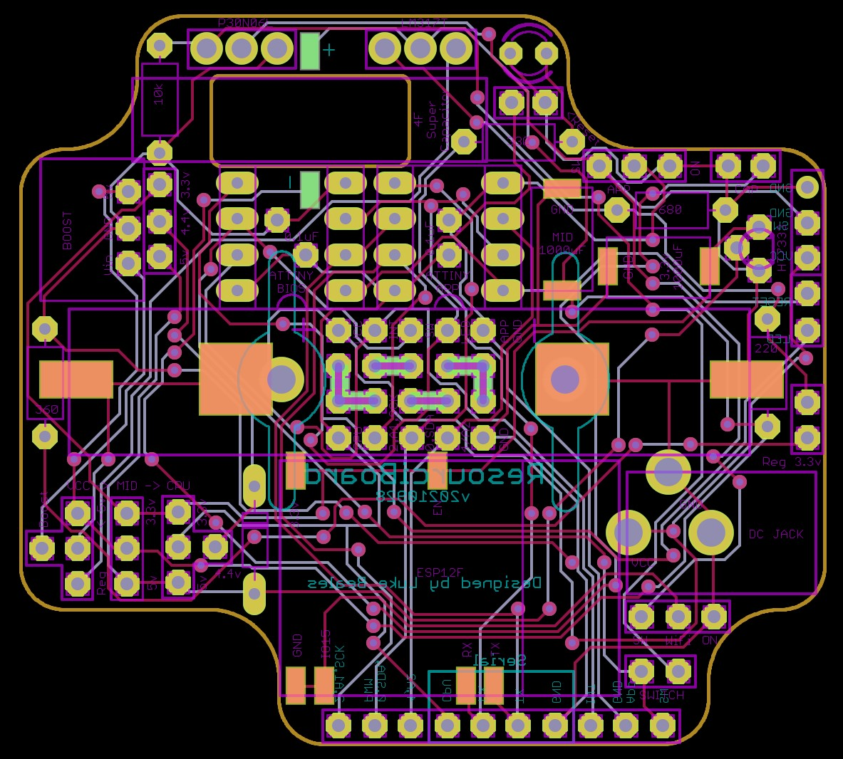
The fit of components seems ok, so now it’s on to seeing if the signals are good. I generated a routed board design to see how it would go.
This has been printed out so now I can do the slow process of checking each line to see if it all connects where it should.
If that all checks out then it’s over to talking to the PCB printers.
It didn’t check out…
I noticed almost straight away that the autorouter in eagle does some odd things. It connected two pins next to each other correctly, but the route went halfway around the board when it didn’t need to. Also I discovered some pins were back to front or could be swapped to be better, and that I didn’t want any Via’s where the ESP12F’s contacts would be. The big issue though was the decoupling capacitors – the traces for it should be directly to the pins – but they went a crazy distance away.
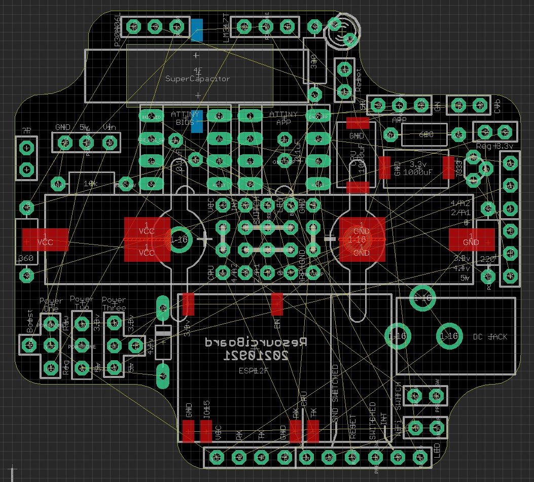
So the trick is to do the short routes first like decoupling capacitors, so you know they will be connected directly. Then run the autorouter for the rest.
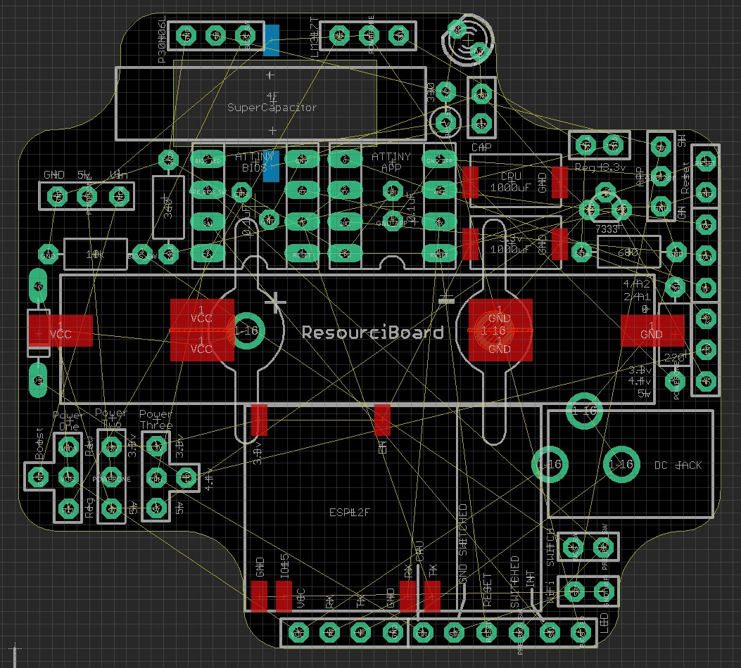
A few more pin swaps and adjustments later, I now have another board to look over and see what else I have missed, but I can sense the finish line!
Ok it turns out I have missed a number of things, so after fixing those up and cleaning up some of the routes, this is the current one. Still a few crazy routes but I can’t do much about them. I am determined to get this done today.

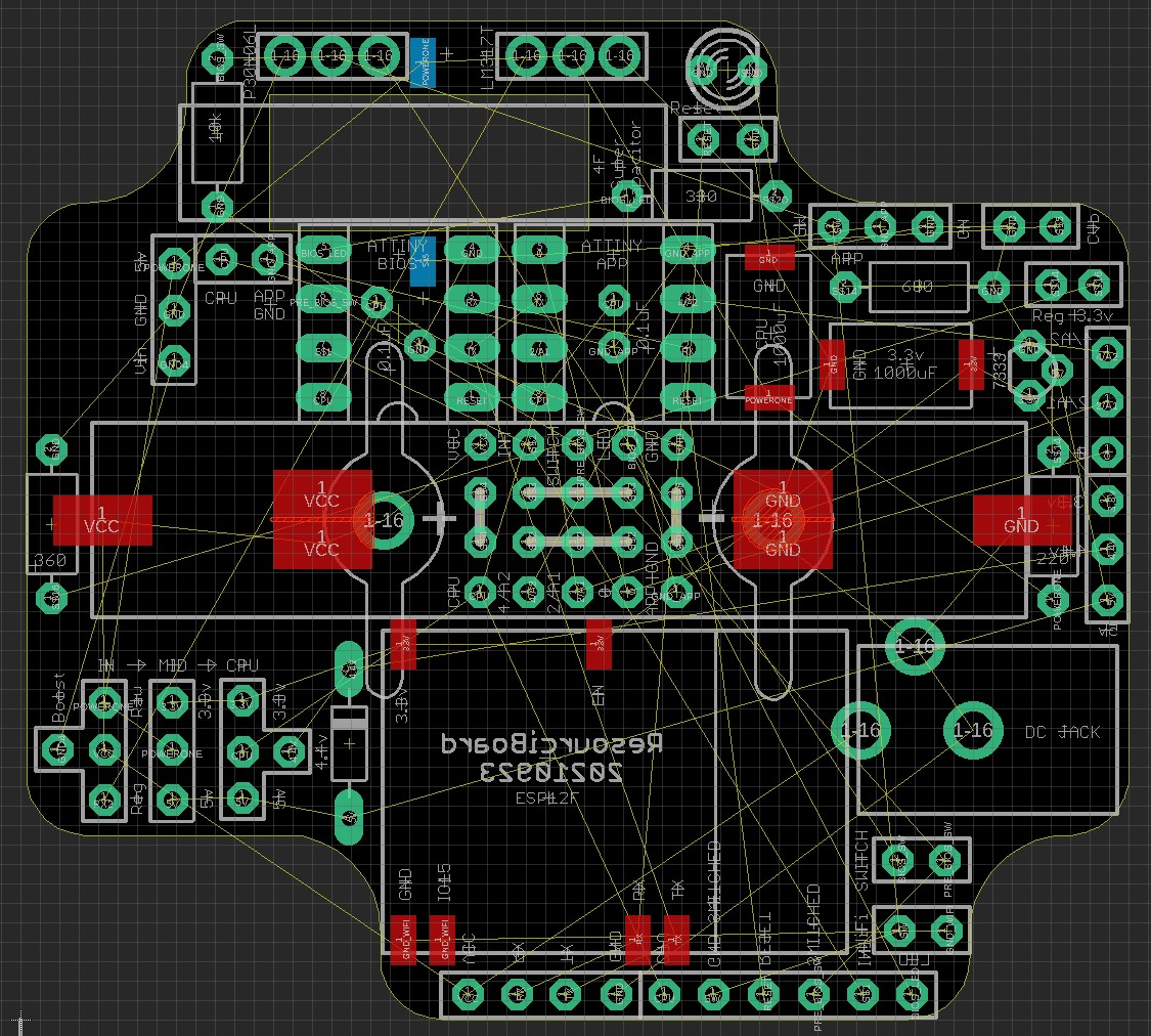
Checking the gerbers
With everything cleaned up and adjusted to meet the manufacturers standards, I now have all the gerber files to double check everything.
All looks good, so it’s now been sent off to the manufacturer! It should arrive in a week or two so I had best get ordering all the individual components.
So that’s all the designing and arranging done. The next step will be to assemble it and check that it all fits, adjust as necessary, test it, etc.
Click here to continue on to Part 3, assembly.